
A scattering type microscope scanning near-field millimeter waves
The aim of the project is to study, realize and validate a vector scanning near-field mm-wave microscope s-(SNMM), which will be very performing in image formation and resolution, on the basis of the fundamental study of advanced micro...

SOIB-project: Groundbreaking opto-electronic semi-conductor devices for CO2 lasers for industrial and medical applications
In this project, work will be done on three components that can be marketed for
laser applications in the industrial and medical world: a Q-switch for a
high pulse frequency pulsed laser, a radial polarizer for high
power laser cutting ...

Infrastructures for broadband wireless/photonic communication and integration of European assets.
Dit project tracht de voordelen van radio technologie (flexibiliteit) en optische vezeltechnologie (capaciteit) te verenigen door te zoeken naar low cost componenten en systeemelementen voor het integreren van draadloze technologie met vezeltechnolog...

Visualisation of hidden objetcs making use of millimeterwave systems
Dit project beoogt in eerste instantie een systeem te bouwen waarmee actieve beeldvorming in het frequentiegebied rond 100GHz van verborgen objecten ken bestudeerd worden. Dit systeem zal o.a. besteen uit een belichtingsblok dat een continu instelbar...

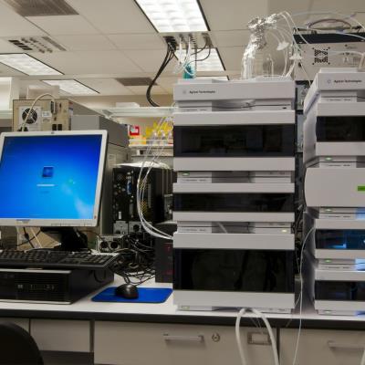
Visualisation of concealed objects using millimetre wave systems
Research in the area of millimetre wave systems is aiming at finding techniques and developing the technology platform to organise a suitable illumination and detection scheme to minimize image noise.
This research project will lead to an experti...

First Aid Kit: Micro-Photonics
In this project two research groups of the Faculty of Applied Sciences of the VUB, namely the department of Applied Physics and Photonics (TONA) the Laboratory for Micro-and Opto-electronics (LAMI), present the fundamental and applied resea...

Active imaging techniques for the detection of hidden objects with electromagnetic waves in the W-band between 75-110 GHz
In this project we study exposure techniques and the necessary components and subsystems for active imaging in the spectrum of the W-band (75-110 GHz). It is a hitherto unexplored area of ??the electromagnetic spectrum in general and for im...
Study, realisation and characterisation of new medium infrared (MIR) sources, modulators and passive components
The project comprises the study of various optical sources and modulators of the wavelength range between 2 and 12 micron.
1/ The challenge is to design an innovative low-voltage modulator (<20V) to allow CO2 lasers to Q-switch (Eng: Q...
Study of opto-elektronic components with the aid of nanometer resolution diffractive gratings
In this project we wish to bundle the know-how of the different participating groups. On one hand we want to tackle our common problem of efficiently coupling light in and out of our optoelectronic devices by studying and using nanometer resolut...

Study of opto-elektronic components with the aid of nanometer resolution diffractive gratings
In this project we wish to bundle the know-how of the different participating groups. On one hand we want to tackle our common problem of efficiently coupling light in and out of our devices by studying and using nanometer resolution diffractive...

Study of opto-electronic components with the aid of nanometer resolution diffractive gratings.
In this project we wish to bundle the know-how of the different participating groups. On one hand we want to tackle our common problem of efficiently coupling light in and out of our devices by studying and using nanometer resolution diffractive...
Photonics in Computing II
This project is about photons and electrons in information technology. It aims at developing micro-optic components and optoelectronic devices that could play a major role in digital optical information processing and switching systems.
Besid...
Research into the effect of nanometer technology on the evolution of integrated circuits. Part I: Components
The use of nanometer technology allows integrated circuits to contain devices and interconnections with dimensions below 0.1 micrometers. People believe power dissipation in devices and interconnect lines will prevent a further down scaling of IC tec...

Generic approach to manufacturable optoelectronic interconnects for VSLI circuits (OIIC)
In this project we want to find solutions to the difficulties of electronic interconnects to handle high thoughput data transfer within and between silicon VSLI chips. The project will demonstrate the advantages of high-throughput optical chip&#...
Components and networks for optically switched broadband communication
There is currently an increasing demand for higher capacity and flexibility in telecommunication networks. One of the key technologies of the future will be optical switching (in space, time and wavelength). This switching can be used inside a switch...
Photonics in Computing
This Project is about photons and electrons in Information Technology. It aims at developing devices, interconnects and architectures for digital optical signal processing. The project is structured in two parts : Part I is an extension of the prese...